
Application note ·
BliXray BLCT-NANOLAB: nanofocus CT for die-attach voids in SiC and GaN devices
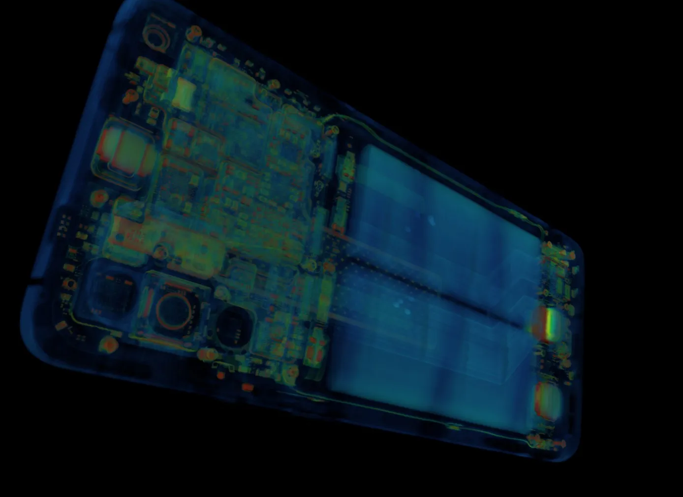
BliXray offers CT inspection of die-attach voids in SiC and GaN power devices with the BLCT-NANOLAB, a laboratory CT system with an open-tube nanofocus X-ray source of up to 190 kV. In its high-resolution configuration, the BLCT-NANOLAB reaches a 2D resolution of 0.5 µm and a 3D resolution of 1 µm. It shows voids, cracks and wire-bond defects inside the closed package, without sectioning the device.
Silicon carbide (SiC) and gallium nitride (GaN) devices carry high power densities in a small die, so the die attach forms the main thermal path from chip to substrate. Voids, cracks and delamination in that layer sit under the die and the moulding compound and cannot be seen from the outside. Computed tomography (CT) with the BLCT-NANOLAB makes this layer visible in three dimensions. In one scan, the system resolves:
- voids, micro-voids and porosity in the die-attach layer
- micro-cracks in the die and in the attach layer
- delamination between die, attach layer and substrate
- bonding-wire and chip-bonding defects
- inclusions in the package
Sub-micron resolution for single devices
The BLCT-NANOLAB is designed for small samples such as discrete devices, dies on substrate and power-module sections. Its open-tube nanofocus source operates from 110 to 190 kV at up to 50 W. The base configuration resolves 2.5 µm in 2D and 3 µm in 3D; the high-resolution configuration resolves 0.5 µm (JIMA) in 2D and 1 µm in 3D.
In nanofocus mode, the BLCT-NANOLAB works with a flat-panel detector of 4608 × 5890 pixels at a pixel pitch of 49.5 µm and an active area of 228 × 291 mm. A focus–detector distance of up to 1000 mm gives high geometric magnification for a die only a few millimetres wide. The system accepts samples up to ø200 × 225 mm and 5 kg in this mode. Measurement accuracy is stated as 3.0 + L/50 µm, and the main frame is made of granite for mechanical stability during long, high-magnification scans.
From the module to the die in one cabinet
The same BLCT-NANOLAB cabinet switches to a 225 kV microfocus configuration for larger parts. In this mode, it delivers 350 W and a resolution of 2 µm (JIMA). A 3072 × 3072 pixel detector with an active area of 427 × 427 mm covers samples up to ø300 × 250 mm and 15 kg. A complete power module or a populated board therefore fits into the same system as the single device.
For failure analysis, this suggests a two-step method. A microfocus overview scan of the module shows which device or bond area stands out. A nanofocus scan of that region then resolves the die attach and the wire bonds at sub-micron detail in the high-resolution configuration. The BLCT-NANOLAB supports circular, helical and segmented scanning, and a jitter scan mode that reduces ring artefacts in the reconstructed volume.
Failure analysis without sectioning
The reconstructed volume shows the die attach slice by slice and in any orientation. Size, shape and position of each void become visible, as does a crack running from the die edge into the attach layer. Wire bonds can be followed along their full length from the die pad to the lead frame. Because the device stays intact, it remains available for electrical testing, for a second scan after thermal cycling, or for a targeted cross-section at the exact position the CT data points to.
“The BLCT-NANOLAB gives a qualification lab a three-dimensional view of the die attach before anyone picks up a saw,” says Adrian de Riz, Managing Director, BliXray Technologies GmbH. “The sectioning that follows is placed exactly where the CT shows a void or a crack.”
Small samples give the best results. A single device mounted close to the source allows the highest magnification, while a full module limits it and is better scanned in microfocus mode first. BliXray scans customer devices on request through its CT testing service, so the data on the actual package is available before a configuration is chosen. Further applications are listed on the electronics industry page, and the full specification is on the BLCT-NANOLAB machine page.
| Parameter | BLCT-NANOLAB |
|---|---|
| X-ray source (nanofocus mode) | open tube, 110–190 kV, up to 50 W |
| Resolution, base configuration | 2.5 µm (2D), 3 µm (3D) |
| Resolution, high-resolution configuration | 0.5 µm (2D, JIMA), 1 µm (3D) |
| Detector (nanofocus mode) | 4608 × 5890 pixels, 49.5 µm pitch, 228 × 291 mm |
| Focus–detector distance | up to 1000 mm |
| Maximum sample size and weight (nanofocus mode) | ø200 × 225 mm, 5 kg |
| Microfocus mode | 225 kV, 350 W, 2 µm (JIMA), ø300 × 250 mm, 15 kg |
| Measurement accuracy | 3.0 + L/50 µm |
| Scan modes | circular, helical, segmented, jitter scan |
“We scan the customer’s own SiC or GaN device and hand over the volume,” says Adrian de Riz. “The engineer then judges die attach and bonds on real data.”
Test scans available
BliXray offers test scans of SiC and GaN devices, dies and power modules on the BLCT-NANOLAB. Contact Adrian de Riz, Managing Director, BliXray Technologies GmbH, a.deriz@blix-ray.de, +49 511 57092696 – www.blix-ray.de.
About BliXray: BliXray Technologies GmbH, Hannover, designs and builds industrial CT systems and X-ray safety cabinets. Manufacturers in defence, aerospace and research use BliXray CT to inspect safety-critical parts without destroying them. BliXray cabinets and containers house X-ray sources up to 300 kV at a protection level of 0.5 µSv/h. CT for critical parts. Shielding for any source.