
Application note ·
High-reliability package CT: BliXray Laboratory CT separates overlapping interconnects
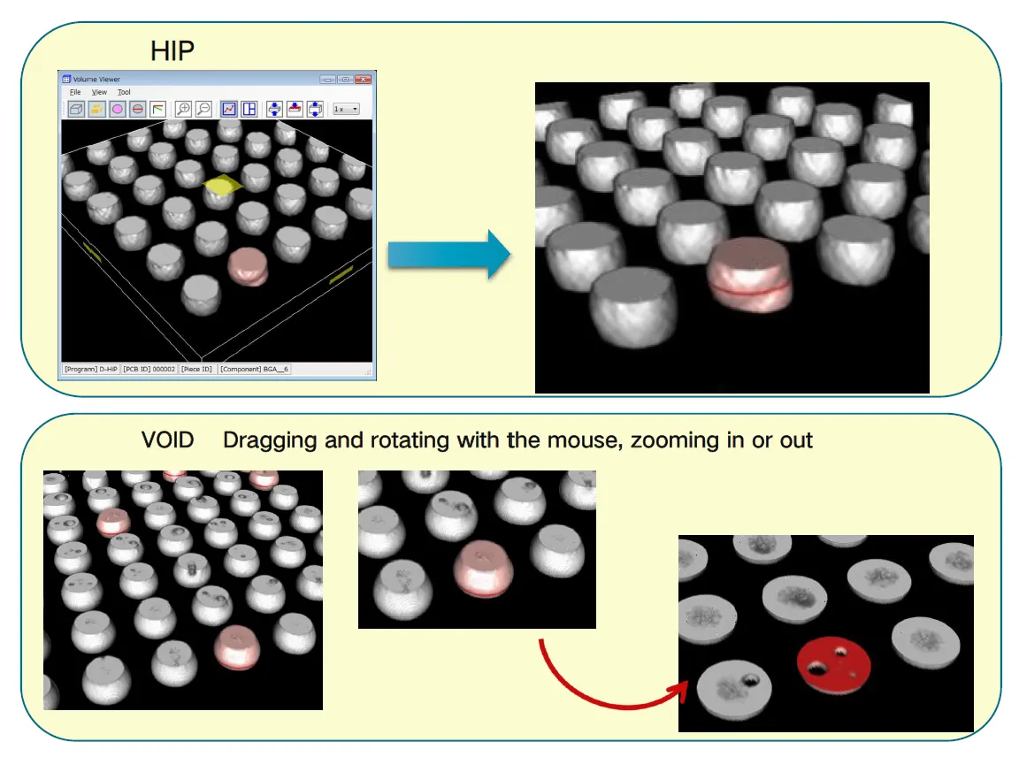
BliXray offers high-reliability package CT with its Laboratory CT systems: one 3D scan separates overlapping solder and interconnect layers in BGA, PoP, QFP, MOSFET and IGBT packages without decapsulation or cross-sectioning. The reconstructed volume shows voids, head-in-pillow joints and wire-bond defects layer by layer, so each joint is judged on its own.
In package-on-package stacks and dense ball grid arrays, the critical joints sit behind other joints, dies and moulding compound. A 2D X-ray image projects all of these layers onto one plane, so a void in the lower ball row and a sound ball in the upper row merge into one shadow. Computed tomography (CT) with BliXray Laboratory CT resolves this overlap in three dimensions. In one scan, it shows:
- voids in solder joints and in the die attach
- head-in-pillow and open joints
- bridging, non-wetting, cold joints and missing or insufficient solder
- misalignment of balls, leads and the package
- wire-bond breaks, lifted bonds, shorts and pitch deviation
Stacked joints separated layer by layer
For BGA and PoP packages, BliXray Laboratory CT reconstructs the complete ball array as a volume. The volume is viewed along three axes – XY, YZ and XZ – and stepped through slice by slice, from the board pad up to the package substrate. In a PoP stack, the lower and the upper ball rows appear in separate slices instead of one combined shadow. A void becomes visible in the joint where it sits, together with its position in the ball.
Head-in-pillow defects show as a thin separating line between the solder ball and the paste deposit on the pad: the two touch but have not merged. In a 2D image, such a joint looks like a good ball. In the CT volume, the line is visible around the circumference of the joint. The volume can be rotated and zoomed, so a suspect joint is checked from every side before a decision is made.
“BliXray Laboratory CT shows each ball of a stacked package in its own layer,” says Adrian de Riz, Managing Director, BliXray Technologies GmbH. “A head-in-pillow joint that looks sound in 2D is visible in the CT volume before the board is cut.”
Leaded packages and power devices inspected inside the mould
The same Laboratory CT method covers QFP packages, MOSFETs, IGBTs and LED packages. For leaded packages, it shows the solder joint under and beside each lead, including non-wetting, bridging between neighbouring leads and missing or insufficient solder. In MOSFET and IGBT packages, the volume shows voids in the die attach under the chip and the path of each bond wire. Wire-bond breaks, lifted bonds, shorts between wires and deviations in wire pitch are followed along the full wire inside the moulding compound. No decapsulation is involved, so the device stays intact for electrical testing or a targeted cross-section afterwards.
For multilayer boards, BliXray Laboratory CT inspects the populated PCB layer by layer without disassembly. Solder joints, vias, traces and bond wires are examined in one volume. A fault in an inner layer is therefore located before any section is placed. Package-level misalignment, such as a shifted or tilted component, is visible relative to the board in the same data.
Quick 2D screening, then 3D CT where it counts
For dense, encapsulated avionics assemblies, BliXray combines integrated 2D radioscopy as a quick screen with 3D CT for deep inspection. The 2D image shows the whole assembly at once and points to the areas that stand out. The CT scan then resolves those areas layer by layer and covers visible and hidden connections alike. This two-step method keeps scan time for the joints where overlapping layers make a 2D decision uncertain.
Small samples give the most detail, because a single package placed close to the source allows higher magnification than a complete board. Large populated boards are best screened as a whole first and then scanned in the regions of interest. BliXray scans customer packages and boards through its CT testing service, so data on the actual part is available before a system configuration is chosen. Further applications are listed on the electronics and aerospace industry pages.
| Parameter | BliXray Laboratory CT |
|---|---|
| Package types | BGA, PoP, QFP, MOSFET, IGBT, LED, multilayer PCB |
| Defects shown | voids, head-in-pillow and open joints, bridging, non-wetting, cold joints, missing or insufficient solder, misalignment, wire-bond breaks, lifts, shorts and pitch deviation, die-attach voids |
| Viewing | multi-axis (XY, YZ, XZ), layer by layer |
| Sample preparation | none – no decapsulation, no cross-sectioning |
| Workflow for assemblies | integrated 2D radioscopy quick screen plus 3D CT deep inspection |
“We scan the customer’s own package and hand over the volume,” says Adrian de Riz. “The failure analysis then starts from three-dimensional data instead of a first cut.”
Test scans available
BliXray offers test scans of BGA, PoP, QFP, MOSFET and IGBT packages and of populated boards on its Laboratory CT systems. Contact Adrian de Riz, Managing Director, BliXray Technologies GmbH, a.deriz@blix-ray.de, +49 511 57092696 – www.blix-ray.de.
About BliXray: BliXray Technologies GmbH, Hannover, designs and builds industrial CT systems and X-ray safety cabinets. Manufacturers in defence, aerospace and research use BliXray CT to inspect safety-critical parts without destroying them. BliXray cabinets and containers house X-ray sources up to 300 kV at a protection level of 0.5 µSv/h. CT for critical parts. Shielding for any source.