
News ·
BliXray brings sub-micron CT to compound semiconductor and gallium production
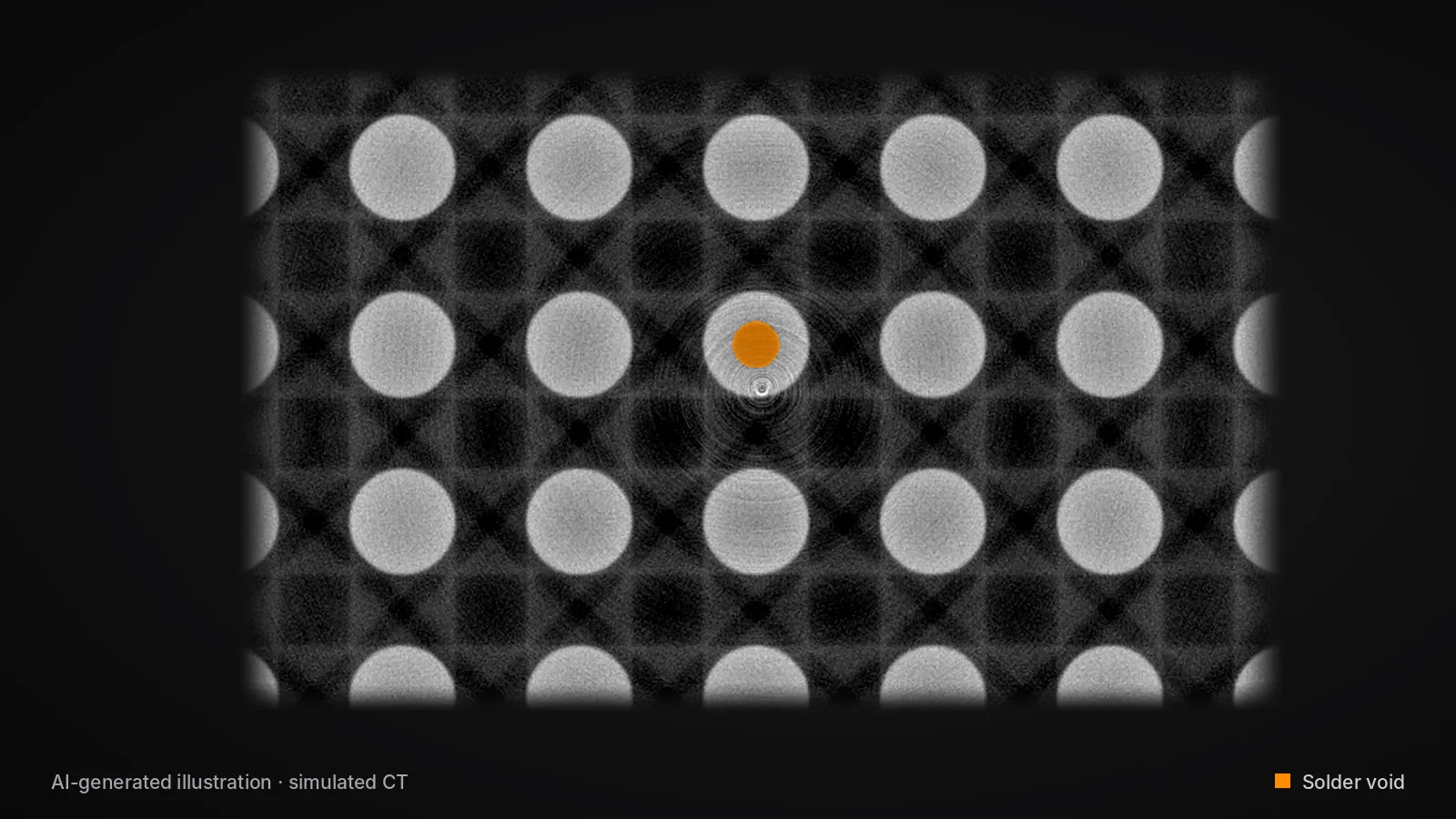
BliXray Technologies GmbH brings sub-micron CT to compound semiconductor and gallium production with the BLCT-NANOLAB, whose 190 kV open nanofocus X-ray source reaches a JIMA resolution of 0.5 µm. For routine checks next to the process, the BLCT-DESKLAB adds desktop micro-CT with a resolution of 3 µm and one-click imaging.
BliXray offers both systems to the compound semiconductor, gallium and related material plants now scaling up in Europe for civil and defence supply chains. Computed tomography (CT) inspects wafers, dies, packaged devices and material samples without destroying them, so every part examined stays available for further testing. The two machines cover the range from single-die failure analysis to quick sampling of incoming material.
- Nanofocus source: open X-ray tube up to 190 kV and 50 W, JIMA resolution 0.5 µm (BLCT-NANOLAB).
- Second configuration: 225 kV microfocus source with 350 W and a JIMA resolution of 2 µm for samples up to 15 kg (BLCT-NANOLAB).
- Desktop micro-CT: closed X-ray tube from 20 to 130 kV at up to 65 W, resolution 3 µm, one-click imaging (BLCT-DESKLAB).
- Scan modes: circular, helical and segmented scans plus jitter-artefact removal.
Sub-micron detail inside the closed package
The BLCT-NANOLAB pairs its nanofocus source with a flat-panel detector of 4608 × 5890 pixels at a pixel pitch of 49.5 µm. In this configuration it accepts samples up to ø200 × 225 mm and 5 kg, the size range of dies, substrates and packaged components. The system resolves micro-voids, micro-cracks, inclusions and delamination as well as bond-wire and die-attach defects inside the closed package. A density resolution of 0.5 % or better separates small density differences within one sample. The same data set shows porosity and inclusions in material samples, which supports the characterisation of compound semiconductor and gallium materials alongside packaging inspection.
“The BLCT-NANOLAB shows a process engineer the void, the crack or the lifted bond wire in a packaged device without opening it,” says Adrian de Riz, Managing Director, BliXray Technologies GmbH. “The part stays intact for every test that follows.”
One cabinet, two source configurations
The BLCT-NANOLAB switches between the nanofocus configuration and a 225 kV microfocus configuration with 350 W and a JIMA resolution of 2 µm. The microfocus configuration works with a 3072 × 3072 pixel flat-panel detector of 427 × 427 mm and takes samples up to 15 kg at a standard scan size of ø300 × 250 mm. One system thus covers failure analysis of single dies and inspection of larger packaged assemblies and carriers. Helical and segmented scans extend the scanned height for tall samples, and jitter-artefact removal keeps fine structures sharp at high magnification. Details are on the BLCT-NANOLAB page.
Desktop micro-CT on the lab bench
The BLCT-DESKLAB is a desktop micro-CT system with a footprint of 1357 × 820 × 900 mm and a weight of 0.9 t. Its closed X-ray tube operates from 20 to 130 kV at up to 65 W and reaches a resolution of 3 µm, with a 2D resolution of 5.8 lp/mm. Scans of samples up to ø210 × 140 mm and 5 kg start with one click, which suits incoming-material checks, process sampling and training. Radiation leakage stays below 0.5 µSv/h. Circular, helical, segmented, offset and limited-angle scan modes cover flat substrates as well as compact samples.
“The BLCT-DESKLAB puts CT on the lab bench for routine checks, and the BLCT-NANOLAB takes the samples that call for sub-micron detail,” adds de Riz.
BliXray supports both systems with installation, training and application advice. More applications are listed under electronics and research.
Test scans available
BliXray offers test scans of customer samples on request through its CT testing service.
Contact Adrian de Riz, Managing Director, BliXray Technologies GmbH, a.deriz@blix-ray.de, +49 511 57092696 – www.blix-ray.de.
About BliXray: BliXray Technologies GmbH, Hannover, designs and builds industrial CT systems and X-ray safety cabinets. Manufacturers in defence, aerospace and research use BliXray CT to inspect safety-critical parts without destroying them. BliXray cabinets and containers house X-ray sources up to 300 kV at a protection level of 0.5 µSv/h. CT for critical parts. Shielding for any source.